Wednesday, May 11, 2011

Capitol Hill Day


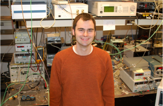
(From Left: Laura Kolton (OSA Public Policy Team), Greg Quarles (President of B.E. Meyers Electro Optics), James van Howe (Assistant Professor, Augustana College), Representative Bobby Schilling (IL), Adam Zysk (research associate IIT, Chicago), Hong-Jhang Syu (Research Assistant, National Taiwan University))


On Thursday May 5th, a number of the conference attendees took a bus to Washington D.C. to visit the offices of various members of congress and senators of our respective legislative districts and states. Our goal was to help defend science funding levels in the wake of strong national sentiment to reduce U.S. federal spending.

What we learned the night before in the briefing at the Baltimore Convention Center was fascinating, and the actual day of visiting policy-makers to discuss science-funding issues was exhilarating. In the briefing, we learned that one of most effective ways of influencing a senator or member of congress was through a conversation with a constituent. Visits from lobbyists actually rank much lower on survey data from congressional staffers. What was also fascinating to me was that an email from a constituent ranked just below a visit from a constituent and still far above a visit from a lobbyist. I immediately promised myself to regularly send email to my representatives and you should too! It works!

At the briefing, one of the speakers, Mike Lubell, the Public Affairs Director at the American Physical Society, showed us revealing survey data from focus groups. One group was from a community with many ties to science industry and one had very little. Shockingly, the results were the roughly the same for each:

1. The groups generally loved science and are supportive of science research
2. The groups thought that science should be a national priority
3. Here's the kicker: The the groups were distrusting of the federal government as the funding source for science research. Somehow they want to keep good science without federal funding.

So there is good and bad news. Scientist can expect good moral and emotional support from the public, but maybe not dollars. In fact, Lubell showed a list that had science as the second most chosen category from the groups of where to cut federal funding.

Our task for the Capitol Hill visits was well laid out- try to educate our representatives about the role of federal money in science research; how it is almost the sole source for science funding in the U.S., how science requires sustained funding over time for results, and how our quality of life is enhanced by the technology we develop such as noninvasive biomedical imaging techniques for cancer diagnostics and photovoltaics for green energy production, not to mention the highly skilled workforce good science creates.

I particularly liked Lubell's list of "good" and "bad" words and phrases to bring up or avoid as you are trying to convince non-scientists of the importance of federal funding for science. Words like "basic research" and "fundamental research" did note bode well in the public eye. They took "basic" and "fundamental" to mean "remedial." The phrase, "Investing in America's future," tracks well with Democrats, but not Republicans since "investment" to the GOP means "spending." There was a fairly strong equal distaste among different parties for the idea that America needs to be the top competitor among foreign nations in science. I guess our Cold War attitude as been slipping since Reagan administration. A "good" party-neutral phrase is the cheesy (sorry but it is), "Building a better America." The list goes on and is both entertaining and illuminating as to the perception of science in the U.S.

Because I live in Iowa but work in Illinois, I met a handful of staffers from both states. From the picture above, you can see that my team was able to personally meet congressman Bobby Schilling (R) from Illinois. Congressman Schilling was extremely kind and hospitable, as were the staffers from the other offices we visited: Senator Kirk (R-IL), Senator Grassley (R-IA), Congressman Quigley (D-IL), and Congressman Braley (D-IA). I was very impressed with the professionalism and cordiality of the young staffers who took the time to listen to our concerns.

So I know you are now asking yourself, "What can I do to help?" Begin by emailing your representatives with your concerns for science funding (at the Capitol Hill visits we were advocating sustained levels (not an increase) . Also be sure to visit the OSA public policy homepage for updates on additional organized Capitol Hill visits, pending science-bearing legislation, letters to sign, etc.

For more info and photos on the Capitol Hill day event click here.

Sunday, May 8, 2011

See you in San Jose!

I hope this post greets everyone safe and cozy at home, resting from a week packed of optics innovation. I am still catching my breath. There was just so much. I would have liked to have attended many more talks, visited more booths at the expo, met up with more colleagues, and posted more (I still might on the latter- it turns out, for better or worse, Newton's First Law applies to blogs as well). Harold Metcalf was correct is is pre-CLEO analysis "Looking over the program and the titles of the sessions, I feel like a kid in a candy store- with unlimited funds, but limited time. It's impossible to do everything."

However, I intend to update this ClEO blog for a little longer with posts that I couldn't squeeze in during the week. I am going to try to have my "candy" and eat it too, though hopefully without a stomachache (figuratively or literally) for blogger or reader.

Regardless, mark your calendars for May 6-11, in 2012 for next year's meeting in San Jose!

Saturday, May 7, 2011

Time-Lens 2.0

Brian Kolner and Moshe Nazarathy coined the word "time-lens" in 1989 after using one to compress a pulse. They made a system in the time-domain that was a complete analog to a lens system in space. Their time-lens took a fat pulse and "focused" it, just like a spatial lens could take a fat beam and focus it to a smaller size. For more details, see Kolner's well-written 1994 review on space-time duality and van Howe and Xu's 2006 review on temporal-imaging devices).

Because much of my thesis work focused (pun intended) on temporal-imaging devices, I can't help seeing them everywhere. This year's CLEO conference was no exception with some talks being more direct about it than others.

Takahide Sakamoto from the National Institute of Information and Communication, in Tokoyo, Japan discussed time-lenses without using the word itself in tutorial, CMBB1, in "Optical Comb and Pulse Generation from CW Light." Sakamoto showed impressive work on comb synthesis from CW light using electro-optic (EO) modulation. He demonstrated that EO phase modulation provides the most efficient way to move from CW light to the picosecond bandwidth regime. Higher order nonlinearities like chi-3 from fiber (EO is chi-2 process) can then be used to move bandwidth to femtosecond regime. Sakamoto stressed a clever biasing and driving technique using an itensity modulator that allowed truly flat comb spectra.

Other work leveraging temporal imaging concepts were CMD1, "Tunable high-energy soliton pulse generation from a large-mode-area fiber pumped by a picosecond time-lens source," from Chris Xu's group at Cornell University and JTuI77, "Scalable 1.28-Tb/s Transmultiplexer Using a Time Lens" by Petrillo and Foster. The former used electro-optic modulation as the time-lens to generate a seed source from CW light for solition shifting. The latter used four-wave mixing as the time-lens mechanism in order to look at the Fourier transform of a data packet for high-speed time-division multiplexing to wavelength-division multiplexing conversion (just as a spatial lens can provide a Fourier transform of a spatial profile, a time-lens can give the power spectrum of a temporal profile). Note that the Xu group has also developed time-lens source for CARS microscopy.

Work from Andrew Weiner's group also made use of time-lenes, CWN3, "Broadband, Spectrally Flat Frequency Combs and Short Pulse Sources from Phase modulated CW: Bandwidth Scaling and Flatness Enhancement using Cascaded FWM" and CFG6, "Microwave Photonic Filters with > 65-dB Sidelobe Suppression Using Directly Generated Broadband, Quasi–Gaussian Shaped Optical Frequency Combs." These works used a front end similar to those shown by Sakamoto, but then added an assisted nonlinear enhancement to bandwidth by using four-wave mixing.

Finally, former CLEO Blogger, Kesnia Dolgaleva, authored CThHH6, "Integrated Temporal Fourier Transformer Based on Chirped Bragg Grating Waveguides" to show a compact, integrated Fourier Transformer, which though not a time-lens, is another device similarly based on space-time duality. This paper draws upon co-author Jose Azana's previous fiber Bragg grating work, which is just one of many Azana's contributions to the field of temporal imaging.

If you look hard enough, you can see time-lenses anywhere- all you need is a device that gives a quadratic phase in time to an optical wavefront (nonlinear frequency mixing, used everywhere in optics, is one technique that works well). However, the big advantage for recognizing a time-lens when you have one is that you can bring all of the knowledge of spatial imaging systems to your work with a simple change of variables.

Thursday, May 5, 2011

The Real-Life Tony Stark


(Robert Downey Jr. plays Tony Stark, defense contractor, billionaire playboy, scientific genius, and alter ego
Iron Man. Image from www.comicbookmovie.com, still from Iron Man 2)

On Tuesday, May 3, I sat in on part of the Market Focus talks at the CLEO expo on defense. The Market Focus sessions cover various business and commercial applications of optics research. Last year was the first time I attended a Market Focus session, and I knew I had to go back. It is a little expo in itself that requires no walking- you to sit down and find out trends and problems that need solving in particular commercial areas. Great fodder for new research ideas!

Although the sessions are broken up into specific talks, what makes these sessions unique is that they turn into a round-table discussion at the end (and even during) the session. They have a more intimate and informal feel than the technical talks and have been organized with a specific agenda of bringing the attendee to a common understanding of the particular market being addressed.

For example, in the defense session, moderator John Koroshetz from Northrop Gruman Laser Systems laid out the logical order of talks to help us get our foot in the door of defense contracting: 1) Science and Technology Development, 2) Product Development, 3) Manufacturing, and 4) The Soldier's perspective. The aim was to help a novice understand the cycle of product development, funding, testing, manufacturing, and end-use, which often cycles back to development for upgrading and enhancing the product into its next-generation phase.

The first speaker, Craig Hoffman, from the Naval Research Laboratory, described science and technology development of infrared imaging systems. He broke up NRLs work in this area by spectral region:

-Visible: 0.4-0.7 microns (high photon energy makes devices tolerant to noise, but scattering makes it bad for imaging through dust or fog)

-Near IR: 0.7-3.0 microns (better for imaging through climate, but resolution gets worse because the wavelength is getting longer; becoming less tolerant to noise)

-Mid-IR: 3.0-5.0 microns (getting very good at seeing through climate, but getting even worse with resolution and noise tolerance; detectors may need to be cryogenically cooled to circumvent thermal noise)

-Longwave: 5.0-14.0 microns (least prone to scattering, worst for resolution and noise)

NRL is looking to piggy back imaging systems in these regions for applications in target acquisition, surveillance, and reconnaissance. The shorter wavelength systems use reflected light to gain information about detail of a target whereas the longer wavelength systems make use of emissive properties of a target to gain bulk properties like thermal imaging.

For example, new thermal imaging systems use mid-infrared light detection to gain detailed information about a target, but also use longwave detection in order to gain a wider field of view. You need both since by themselves the former sacrifices field for resolution and the latter sacrifices resolution for field.

Hoffman went on to describe military imaging problems that need better answers 1) Detailed target identification. You don't want to just know if a target is a tractor or a tank, but exactly whose tank it is (friend or foe?) and with enough time to either make evasive maneuvers or decide how to engage. 2) Fast data acquisition for reconnaissance. For this application, you want to collect data from an aircraft that is flying high and fast. You don't have the burden of real-time analysis like target acquisition (you can spend weeks later to analyze data), but you do need to collect enough information, with enough quality during the short acquisition time. 3) Surveilling a small area for weeks on end to look at changes in patterns like traffic flow, building construction, etc.

Hoffman spoke briefly about things like SWaP- size, weight, and power. This acronym represents all the things that should be as small as possible for a viable military product. Pete Vallianos from N2 Imaging systems followed up Hoffman's talk with more of the parameters, tests, and requirements related to SWaP. Vallianos underscored the importance of practicality and robust requirements when it comes to making products for the military. He repeatedly reminded the attendees that the military is not interested in your research per se (definitely not technology for its own sake), but rather interested in how technology might solve problems. While being developed, it needs to go through a variety of rigorous tests- one of the stress tests from the Marines is dropping your product from a height of six feet onto a piece of plywood . If it doesn't survive, it's back to the drawing board.

Vallianos described some specific product development interests of the military in imaging:

-microbolometers
-small eye safe lasers
-CMOS, low level light detection
-lightweight visible optics
-high transmission in optics across the visible spectrum through the longwave IR
-moldable aspheric lenses
-robust broadband optical coatings
-OLEDs
-LCDs
-Lightweight optical "network" on a soldiers back
-Any decrease in power for powered optics to get grid of as many of the batteries as possible a soldier needs to carry in his or her pack.

Though the speakers did not describe any iron suits with flying capability, or magic cold-fusion-like power supplies, I think Tony Stark still would have been proud of this session.

Post-deadline Prep

Just wanted to chime in with a nagging note to remind you to plan your post-deadline itinerary before 8 pm. I am going to commit to PDPA-Session I and not try to hop around the standing-room only crowd. I am particularly interested in the supercontinuum generation and frequency-comb work in this session, some of which is pushing into the mid-ir where there are interesting chemicals to identify for spectroscopy and stand-off detection. Other broadband generation in this session has been performed with small waveguides or micro-resonantors- little pocket combs on silicon (see the April 20, post for more details). I will be disappointed to miss the new Applications and Technology Session, particularly the biomedical work. These groups by far always have the coolest pictures, images, and videos. If you can make it to these talks, the first four of PDPB-Session II, be prepared to be blown away by beautiful videos and images that address improving image acquisition rate, penetration depth, and resolution (again, see the April 20, post for more details). Very likely, these state-of-the-art techniques may be used on you in your lifetime. You can tell your doctor, "I saw this work at CLEO 2011 before you even graduated from med school."

Wednesday, May 4, 2011

The Romance of Photonic Lattices and Ham

(Left: beam profile in one of Mordechai Segev's 2D photonic crystal lattices. The transverse disorder increases from c) to e). From Schwartz, Segev et al)

This year's CLEO plenary sessions were exceptional. Monday evening hosted talks by Donald Keck, who pioneered the first low-loss optical fiber and James Fujimoto, renown for developing optical coherence tomography. Wednesday morning's plenary followed with exhilarating work (I'm serious, not just blogger hyperbole here) on photonic crystals. Even the awards were exciting. Amnon Yariv, responsible for the creation of the distributed feedback laser, and whose book "Optical Electronics in Modern Communication," I safeguard as one of the most helpful optics texts on my shelf, was presented with the 2011 IEEE Photonics Award. In his acceptance speech, he spoke briefly of his emigration to the United States from Israel 60 years ago. The freighter that carried him, other passengers, and iron ore across the Atlantic, made entry in none other than the city of Baltimore. Yariv, reminisced about his first meal after landing in a gritty, industrial, 1950s Baltimore-a ham sandwich (his first ever)!

After the awards, the plenary speakers Mordechai (Moti) Segev and Susumu Noda spoke about their respective work on photonic crystals. Segev, a charismatic speaker, setup a beautiful story addressing a fundamental understanding of periodic and random structures via photonic lattices. He specifically spoke about work on Anderson Localization of Photons, the optical analog to Anderson's Theory for Localization of electron's in a crystal lattice. By introducing disorder into a 2D photonic lattice, Segev was able to constructively interfere light over a small area, and destructively interfere light everywhere else. Diffraction is thwarted, analogous to how diffusion is thwarted by the interference of electron waves for Anderson Localization in a crystal lattice (see figure above). Check out Frank Kuo's February 26, blogpost with more details describing this work.

Segev's group of course has pushed this work further, and into stranger directions. In contrast to confinement, Segev's group found that they could make a beam expand faster than diffraction, hyper-transport. One reason this work is so beautiful is that the theory and phenomena for photonic lattices can be borrowed from crystal lattices in condensed matter and visa-versa. The equations are the same, you just need to change the variables and some good creativity. In 2008, Roati et al leveraged work from Anderson Localization in photonic lattices to demonstrate Anderson Localization for the first time using matter waves. This makes me wonder about a designing a crystal structure with say hyper-diffusion? With a sharp mind and good imagination, the possibilities seem endless.

Segev does a fantastic job framing his work romantically. Though the devices his group makes have great practical implications, it is all through the guise of exploring the nature of world. Segev helps remind us why we became interested in science in the first place, for the thrill of exploration and finding answers, to generate new questions, and to pursue things because they are beautiful.

Segev was a tough act to follow, but Noda came through. After Segev's nice setup, Noda showed one impressive photonic crystal device after the other. Here is a list of some of the groundbreaking devices he has made:

-Nano-cavities with Q > 40,000
-Inhibition of spontaneous emission
-Light that can make right angle turns
-Slowing or stopping light with probe pulses
-Novel gates for quantum computing
-Small beam-steering devices
-High-efficiency, high power single wavelength emitters
-Creation of unique beam patterns for applications like optical trapping of non-dielectric particles
-Sub-wavelength focusing of beams
-Thermal emission control (shaping and redistribution of blackbody spectra)

Again, for details on the physics behind some of these devices, see Frank Kuo's February 26, blogpost. I left this plenary session inspired, ready to get into the lab to get some work done, and strangely with the craving for a Baltimore ham sandwich.

Tuesday, May 3, 2011

Lasers can Mold and Manipulate Metal as easy as Play-doh

(Left: Dr. Marshall Jones from GE Global Research; Photo from GE)

The head of the student machine shop at Cornell, Bob Snedeker ( Sned), liked to remind us in a sarcastic fashion that its easier to take material away from a workpiece than to put it back on- warning: be careful about how much you take off as you cut. Or as the old saying goes in carpentry, "measure twice, cut once." This is not necessarily true for laser machining of metals. Laser cladding, which was one of the topics discussed in the tutorial, AMB1 "Industrial Applications of Laser Materials Processing," by Dr. Marshall Jones from GE Global Research, is a technique in which material can be added to a workpiece where too much was accidentally cut off. Like Play-doh, you can just put back on what you need. Wow, if only I could have laser-cladded my tool bits, and special nut and bolt we were required to make in order to graduate from machine-shop training! Sned had high standards and we spent many hours to make a piece to find out we needed to start over with fresh stock. It was back to the grindstone (literally!) until those bits had a perfect angle and facet.

GE uses laser cladding to clean up mistakes that may have been made for particularly expensive pieces such as airfoils for aviation. You don't want to throw these out and start over. Laser cladding is also used for coat metals with another protective metal surface- hardfacing.

Another laser processing technique explained by Marshall was laser-shock peening. Peening (as in a ball peen hammer-a remnant tool from days of blacksmithing) is a technique that reduces the fatigue of a metal (like preventing cracks from spreading) by applying a compression force to the surface. In the old days, this was done with a hammer, Marshall uses a "laser hammer." To create a shock wave powerful enough to peen, you need a laser beam with an a power density of 1010 W/cm2 and an interaction time with the surface of no more than 10 ns. Using an interface like water, through which the compression force propagates to reach the metal surface, can make peening more effective. GE also uses shock peening for aviation pieces in order to extend the life of a particular part.

Marshall also discussed a handful of additional applications for laser welding at GE. GE rail uses laser welding for their diesel engine heads and liners. Their consumer division uses it to weld electrodes of ceramic metal halide lamps- the ones that give a nice white-light spectrum crucial for lighting for retail. Marshall brought up the fact that jewelers and clothing retailers particularly need white-light illumination in their stores to ensure customer satisfaction (you don't want what you thought was a red dress to turn out to really be magenta when you leave a shop and get out into the sunlight). The ceramic metal hallide lamp electrodes are particularly tricky to weld together because of the need to join odd materials W:Mo welds and Mo:Nb welds. GE uses a special three-beam laser system to join these materials.

Finally, Marshall briefly discussed the laser systems themselves used for such applications. The conventional lasers used for processing are CO2 lasers and Nd:YAG systems that give out approximately 20 kW average power. Unfortunately they have 10% and 3% wall-power efficiency respectively, and CO2 lasers require expensive specialty fiber for coupling due to the long emission wavelength. Ytterbium-doped fiber lasers and ampliers are beginning to replace these current workhorses due to high wall-power efficiency, 30%, and all-fiber configurations (zero optical alignment and high flexibility in footprint and beam delivery). The main disadvantage to high-power fiber lasers is expense. However, as fiber-systems continue to be developed, they may very well replace their bulk system competitors in the near-future.

Monday, May 2, 2011

Small, Mountain-Town Mecca for Optics Research


(Above: Big Sky Laser series compact Q-Switched, Nd:YAG from Quantel Laser. Author's note: may not be best to combine beautiful Montana stream with Nd:YAG)


I am likely showing my naivete as a "young" optics researcher, but after my Super Shuttle ride from the airport to my hotel last night, I felt compelled to say something about Bozeman, Montana. And no, I'm not being paid by Bozeman's Chamber of Commerce (though if you are paying attention Bozeman, an all-expenses-paid visit to Bozeman could convince me to write more about your town whose combination of optics innovation and gorgeous backdrop is causing me to want to pack up my bags and head out West to Big Sky Country.)

What peaked my interest about Bozeman were two passengers in my Blue Van who were employed by Bozeman optics companies. I knew ILX Lightwave was out of Bozeman, but didn't realize that was just the beginning. One of the passengers was an HR rep from Quantel. Note to job seekers: Quantel-Medical, which makes laser systems for ophthamology and dermatology, is looking to fill several positions. Find out more information at the CLEO Job Fair.

My surface internet searching led me to make a stab at a list of photonics companies in Bozeman (a booth number adjacent lets you know that they will be at the expo which opens at 9:45 am tomorrow):

AdvR (booth 1330)
Altos Photonics (booth 1225)
Bridger Photonics
ILX Lightwave (booth 1808)
Lattice Materials
Resonon
S2
Scientific Materials Corp
Quantel (booth 1903)
Quantum Composers

This list, which is by no means complete, is still very impressive given that the population of Bozeman is just under 40 thousand.

So why all the optics in Bozeman? A 2005 article from the Bozeman Daily Chronicle gives credit to Montana State University professors Pat Callis and Rufus Cone for strengthening the optics program in the late 1980's which led the establishment of a handful of companies in 1990, such as ILX Lightwave, Big Sky Laser (now Quantel), and Lattice Materials. To further the growth of optics at MSU and colloboration between industry, OpTec was created in 1995 as a multidisciplinary center for optics research. In 1999, Spectrum Lab was formed to specifically transition photonics research from MSU to Montana companies. Bozeman companies have also been no strangers to Small Business Innovation Research (SBIR) grants to bolster the development of optics start-ups.

Be sure to stop by the Bozeman contingent at the expo, if not to talk optics and photonics, at least to hear adventures of fly-fishing, downhill skiing, rugged hiking, and glacier climbing!