Monday, April 25, 2011

Photonic Spark Plugs: Zero to Ten Millijoules in just a Nanosecond


(Prototype of a photonic spark plug using Q-switched Nd:YAG/Cr
4+:YAG microlasers (top), and a standard automobile spark plug (bottom). Photo from
Takunori Taira, National Institutes of Natural Sciences, Japan)

An April 20, CLEO press release recently caught the eye of the BBC News, and with good reason. A Japanes and Romanian collaboration will show data at CLEO from a 10 mm, multi-beam, ceramic laser whose beams can reach energies greater than 10 millijoules over a 800 picosecond pulse width, to ignite fuel for internal combustion.

The research behind the photonic spark plug will be presented in, CMP1 “Composite All-Ceramics, Passively Q-switched Nd:YAG/Cr4+:YAG Monolithic Micro-Laser with Two-Beam Output for Multi-Point Ignition” on May 2, at 1:30 pm, by Takunuroi Taira and Matsaki Tsunekane from the Laser Research Center in Okazaki, Japan, in collaboration with Kenji Kanehara from Nippon Soken, Inc. in Japan, andNicolaie Pavel of Romania’s National Institute for Laser, Plasma and Radiation Physics in Romania.

There are a handful of advantages to using photonic spark plugs over conventional spark plugs. A photonic spark plug could potentially ignite leaner fuel mixtures (more air and less fuel) to reduce emissions of polluting nitrogen oxides (NOx). Conventional spark plugs cannot practically accomplish this right now because the increased spark-voltage required to ignite lean mixtures erodes the electrodes too quickly-they need to be replaced too frequently which is expensive.

Additionally, a photonic spark plug could improve combustion efficiency for better driving performance and/or fuel economy. A conventional spark plug sits on top of the head of a cylinder and ignites the fuel mixture near the top where there is a large thermal mass of cold metal from the cylinder. Taira's photonic spark plug can focus the beams into the center of the gas mixture for three times faster, and a more symmetric, expansion of the flame. Also, the ignition time-scale using the pulsed micro-laser beams is nanoseconds compared to milliseconds for a conventional spark plug. The ability to better control ignition timing over an automobile's cylinders will result in more power delivered to the drive-train when desired.

The Japanese and Romanian collaboration is already working with DENSO Corporation, an affiliate of Toyota. Keep your eyes out for photonic, fiber-patch cord jumper cables in the near future!

Wednesday, April 20, 2011

Postdeadline Papers show Emphasis in Broadband Light Generation, Biomedical Imaging, and Nanophotonics

(Fig. 1 From P. Del'Haye, Nature, 450 1214, (2007). a) frequency comb spectrum, b) degenerate and non-degenerate four-wave-mixing among cavity modes, c) SEM image of torroidal microcavity)

On Thursday May 5, from 8pm- 10pm, conference goers will be madly dashing from ballroom to ballroom to hear the latest breaking optics research- it's like a geeky Black Friday for optical science. There are 36 talks in total, but because they are spread out among three sessions, you realistically can only hear 12. Trying to see more requires cat-like agility to maneuver around standing-room-only crowds. Good thing postdeadline abstracts were recently posted. Be sure to look through the agenda of sessions and plan your evening.

This year's sessions include record breaking feats typical of CLEO postdealine papers: an ultralow 181 nA lasing threshold in a nanocavity laser (PDPA1), a whopping 4176% W-1cm-2 conversion efficiency for parametric fluorescence in a diode laser (PDPA3), a limit-pushing 1.5 mm imaging depth in a mouse brain cortex using a two-photon microscope (PDPB3), Mid-IR to keV X-ray supercontinuum generation (PDPC12), a noise figure less than 3 dB in a phase sensitive amplifier (PDPB10), and many others.

Though the sessions will host a wide variety of topics in fundamental and applied optics, some themes that emerge from this year's postdeadline abstracts are papers that demonstrate broadband frequency generation, biomedical imaging (the postdeadline subcategory CLEO: Applications & Technology 1: Biomedical has the most papers of the three sessions), and nanoscale lasers and nano-photonic devices.

One of the papers on broadband frequency generation, PDPA4, "Mid-Infrared Frequency Combs Based on Microresonators," by Wang et al. from a German, Swiss, and French collaboration (note one of et al's s is Nobel Laureate Theodor Hansch), builds on previous work reported in a 2007 Nature paper to produce a monolithic comb generator in the Mid-IR. The reason for the microresonator is to get rid of the big Ti:Sapphire laser typically used to generate frequency combs in order to scale down cost, complexity and size of the comb generator. The high-Q microresonator, an example of which is shown in the Fig. 1, requires a simple CW pump. Besides being smaller, simpler, and potentially much cheaper, the microresonator has the advantage of producing comb spacings greater than 500 GHz (something unattainable by comb generators that use ultrafast pulsed seed sources like the Ti:Sapph).


(Fig. 2 From Daylight Solutions, interesting molecules arranged by peak absorption wavelength)

One compelling reason for building a comb generator in the Mid-IR is for ultrasensitive, broadband spectroscopy in an interesting spectral region for which there is a dearth of laser sources. Figure 2. from Daylight Solutions (CLEO booth 1526), a company that fabricates quantum cascade lasers between 3.0 and 20.0 microns, sorts molecules of interest by their peak spectral absorbance. These molecules are interesting for environmental monitoring (ozone, water, methane, carbon dioxide), threat and standoff detection (TNT, TATP, VX), and biomedical spectroscopy (glucose).

Similar to the European group's comb generator, PDPA6, "Octave-Spanning Supercontinuum Generation in CMOS-Compatible Silicon Nitride Waveguides, by Halir et al. (Recent MacArthur fellow, Mihal Lipson, is one of the notable et al's on this paper) uses a nanoscale structure, a silicon-based waveguide, to generate an impressive 1.6 octave bandwidth up to 2025 nm on a CMOS compatible platform. Your plug-and-play supercontinuum source is just around the corner! But will it be Windows 7 compatible?

Other postdeadline papers concerned with broadband frequency generation are PDPA5, "Self-Referenced Frequency Comb from a Tm-fiber Amplifier via PPLN Waveguide Supercontinuum," PDPA7, "Spectral Line-by-Line Pulse Shaping of an On-Chip Microresonator Frequency Comb," PDPC9, "Supercontinuum Generation with Self-Healing Airy Pulses," and PDPC12, "Bright Coherent Attosecond-to-Zeptosecond KeV X-ray Supercontinua."


(Fig. 3. From Kobat et al., Optics Exp., 17, 13354, (2009). a) Two-photon image of a mouse cortex with 775 nm excitation and 1280 nm excitation. b) Attenuation of fluorescence vs. depth for 775 nm and 1280 nm excitation.)

New additions to this year's postdeadline session are subcategories in CLEO: Applications and Technology, most notably CLEO: Applications & Technology 1: Biomedical. The four papers in this subcategory demonstrate pushing the limits on resolution, high-speed image acquisition, or penetration depth for different microscopic techniques. PDPB3, "In vivo two-photon imaging of cortical vasculature in mice to 1.5-mm depth with 1280 nm excitation," by Kobat et al. shows record imaging depth in a mouse brain cortex using two-photon microscopy by cleverly using long-wavelength excitation. Typical two-photon microscopes use 800 nm, ultrafast pulses from a Ti:Sapphire laser to excite the tissue to be imaged. Photons may not make it to the depth of interest because of absorption or scattering. In brain tissue, scattering dominates over absorption between 350 nm -1300 nm. By using a longer excitation source, more photons can make it to the target allowing for deeper imaging.

Longer wavelength excitation also means longer wavelength emission, for which there is a decreased absorption due to intrinsic tissue. So by using a 1300 nm excitation source, photons scatter less on the way to the tissue to be imaged, and are absorbed less as the fluorescence makes it way back to the objective lens. Resolution is decreased because of the the longer wavelength, however, tissue can be imaged significantly deeper. Figure 3. shows the difference in image depth using 1280 nm excitation as opposed to 775 nm excitation in the authors' previous 2009 work for which they showed 1.0 mm imaging depth.

These are only some examples of the hot research to be presented at the postdeadline session. After all, there were only 36 accepted papers (they're all hot). Make sure to wear a good pair of shoes, maybe do some some pre-stretching, but most importantly, plan out your postdeadline itinerary by looking at the abstracts. This is one venue where you can be assured every conference attendee will be present.

Thursday, April 7, 2011

Civic Scientific Duty

This is just a short note to emphatically urge any U.S. citizens attending CLEO to sign up and participate in Capitol Hill Day during Thursday May 5, at the CLEO conference. The deadline for signing up is this Friday, April 8. OSA will arrange for you to meet with your district's or state representative(s) so that you can describe the importance of the optics industry, optics and science research, and science education for your state. Your voice is particularly important to prevent harmful or devastating budget cuts to optics, as U.S. congress focuses on ways to cure a ballooning U.S. deficit through budget cuts. Though we may be on different sides of the political aisle, we know that government funding for science research is intimately intertwined with private sector development of cutting edge products. If science and tech funding agencies like NSF, NIH, DOE, DOD, DOC, even USDA (see December FTTH post) take a blow, not only those in academia and government labs will feel it, but the optics industry will as well

OSA will provide training on Wednesday, May 4, at 6 pm for strategies on how to efficiently and appropriately promote science funding to your representatives. On May 5, transportation will be proviced to D.C. via a charter bus. The bus will leave at 8:30 am and return before 5 pm. Because many CLEO attendees might not wish to miss a full day of talks (or might have a talk themselves), OSA recommends the use of a commuter train line from D.C. to Baltimore for those who need to return early.

This is a unique opportunity for scientific civic engagement. Please participate and help keep funding in the optical sciences.

Tuesday, April 5, 2011

Candy store for Lasers and Electro-Optics


(Above: Video Interviews with Program Chairs: from CLEO website)

If you haven't been to the CLEO 2011 conference website in the last week (or even if you have), it is worth taking a look at the video interviews with the programming chairs. There are 11 videos addressing the chairs' top picks for talks, their views of trends in optics, advice for conference goers, and their impressions of CLEO's scope and impact for optics research.

In the interviews, the chairs spoke in unison of how CLEO is unique among optics conferences in its breadth of research, particularly spanning basic research to market-ready products. On one hand, you can find talks on fundamental quantum mechanics such as those in the Symposium on the Zeno Effect in Optoelectronics and Quantum Optics whose subject delves into the fundamental nature of measurement. The quantum Zeno effect (or paradox) refers to inhibiting quantum transitions by frequent, repeated measurement. For example, observing an unstable particle in an undecayed state collapses the wavefunction to this state. By quickly measuring it again and again, you can force the wavefunction to repeatedly collapse to the undecayed state by never giving it time to evolve. It never decays, analogous to how Zeno's arrow never hits its mark. So, how could this be used for quantum optics? Besides generically controlling quantum coherence or decoherence of a system, the quantum Zeno effect has applications in optical switching.

On the other hand, in session "Laser Micro and Nano Structuring", in CLEO: Technology and Applications: Industrial, Guido Hennig from Daetwyler Graphics AG, will give an invited talk, AMD4, "Laser Microstructuring and Processing in Printing Industry," discussing the use of high-power fiber lasers for engraving printing plates, as well as high-speed laser modulation for laser-induced ink transfer. In one of the video interviews, Harold Metcalf, from SUNY Stoneybrook, CLEO:QELS Fundamental Science General Co-Chair, aptly characterizes the wide scope of such interesting topics. "Looking over the program and the titles of the sessions, I feel like a kid in a candy store- with unlimited funds, but limited time. It's impossible to do everything," quips Metcalf. To view the "candy store" selection, which I highly recommend as a way of searching for interesting talks you might otherwise miss, go to the conference itinerary planner and click on "Search" and then the "Session Title" drop down menu. You'll be overwhelmed, impressed, and excited.

Some of the specific goodies highlighted by the program chairs in the video-interviews were contributed papers and invited talks discussing UV LEDs, photovoltaics, nanoscale laser sources, metamaterials, broadband spectroscopy, and integrating optics on-chip. Christian Wetzel of Rensselaer Polytechnic Institute, CLEO: Applications and Technology: Industrial Subcommittee Member, points to tutorial ATuD1, "Water and Air Treatment Using Ultraviolet Light Sources," by Gord Knight of Trojan Technologies, as well as invited talk AMC4, "New Concepts and Materials for Solar Power Conversion Devices," by Wladeck Walukiewicz, of University of California, Berkeley, both of which use group III nitride materials in unique ways to develop "green" photonics (Walukiewicz will discuss inserting another band gap within a band gap to increase solar cell efficiency). Seth Bank of University of Texas at Austin, CLEO: Science and Innovations 3: Semiconductor Lasers Alternate Chair, discusses how this year marks the "emergence of the the nanolaser" and recommends tutorial talk CTuG1, "Nanoscale Lasers: How Small Can they Go?" from Shun Lien Chuang of University of Illinois, Urbana-Champaign as well as device results from invited paper CTuG2, "Room Temperature CW Operation of Metal-Semiconductor Plasmonic Nanolasers with Subwavelength Cavity." Tim Carrig of Lockheed Martin, CLEO: Science and Innovations General Co-Chair, and CLEO: Applications and Technology General Chair, projects now will be the time that companies need to look at the fundamental research on optical metamaterials to begin understanding how to make market-ready products in the near-future. For introductory information on metamaterial applications, a good place to start will be tutorial QTuM1, "Optical Metatronics" from Nader Engheta from University of Pennsylvania.

The suggestions of talks and lists of recommendations from the chairs goes on. To find out more, click on the program chair video link on the CLEO main page.

Thursday, March 17, 2011

CLEO Technology Sparks Controversy

(Left: Data points from Osram Opto Semiconductor of Germany. Lower black square at 142 lm/W demonstrating record white-light LED efficiency; second black square at 160 lm/W shows projected efficiency after further optimization.)

You may not think that LED lighting would be a controversial topic, but as the New York Times reports, it may be indirectly responsible for new anger among conservative lawmakers in the United States. A U.S. federal law passed in 2007 by the Bush administration will, among other energy-saving measures, make the sale of the incandescent 100-watt light bulbs illegal in 2012. Republican representatives Joe Barton of Texas and Michelle Bachmann of Minnesota, and Republican Senator Rand Paul of Kentucky have recently become vocal about the rights of Americans to purchase lighting of their choice (energy-efficient or not).

The alternatives to the more-than-a-century-old technology spurning this debate are a new make-over of halogens (not much more efficient than incandescent bulbs at about 20 lumens/W), compact fluorescent bulbs (about70 lumens/W), and LED lighting (Osram Opto Semiconductors of Germany just recently claimed to have set a record for warm-white LED chips at 142 lumens/W). CLEO attendees beware: might tea-party members be planning protests of sessions within CLEO Science and Innovation 15: LEDs, Photovoltaics and Energy-efficient ("green") Photonics?

The "controversial" talks related to LED lighting can be found specifically in sessions "Nano-structured LEDs" on Monday, May 2, 1:30-3:15 pm and "Toward More Efficient Visible LEDs" on Wednesday, May 4, 1:30-3:10 pm. Many of these talks will address specific problems in the overarching goal of fabricating highly-efficient LEDs that can simultaneously mimic the white-light spectrum of an incandescent light bulb. White-light LEDs could reach luminous efficiencies of greater than 300 lumens/W once certain device and fabrication challenges are overcome.1

One of the greater challenges is overcoming the emission gap in the green-yellow region of the visible spectrum (515-600 nm).1,2 Whether multiple LEDs of different color are combined to produce white-light, or one or two different colored LEDs are used to pump phosphors to produce white light, current designs lack efficient production of yellow-green photons for true white-light color (a stinging irony for a technology slated as "green" photonics). Invited talk, CMU5, "Nitride-based Nano-columns and Applications" and contributed paper CMU6, "Diffraction-Coupled Plasmon-Enhanced Light Emission from InGaN/GaN Quantum Wells" in session "Nano-structured LEDs"will show different approaches to generating green light using nano-structures on InGaN. Lowering the dimensionality by using nano-structures allows one to play with defect, strain, and polarization properties of the material and hence light generating capability and extraction.2

Another challenge being addressed in session "Toward More Efficient Visible LEDs" is "efficiency droop" particular to InGaN. InGaN LEDs show great promise at low currents, but suffer an enormous efficiency reduction (the droop) at high-current injection, a problem for potential use in high-power applications. The jury is still out on the cause for the droop.2 Contributed paper CWF3, "On the symmetry of efficiency-versus-carrier-concentration curves in GaInN/GaN light-emitting diodes and relation to droop-causing mechanisms" will be presenting evidence in support of carrier-leakage theory for droop. Contributed paper CWF4 "Efficiency Droop Reduction in InGaN/GaN Light-emitting Diodes by Graded-thickness Multiple Quantum Wells" will show work demonstrating droop reduction by inserting clever nano-structures into the design.

Whether or not you personally believe you should have the right to buy old-tech, 100-Watt incandescent light bulbs, one thing that is not a controversy is that LED technology is hot. It will likely be the future of lighting for illumination and displays. Don't miss out on these talks.

References

1. E Schubert and J.K. Kim, "Solid-State Light Sources Getting Smart," Science, 308, 1274-1278, (2005).

2. M. Crawford, "LEDs for Solid-State Lighting: Performance Challenges and Recent Advances," J. Sel. Topics in Quant. Electron., 15,
1028-1040, (2009).

Monday, March 14, 2011

Thoughts go out to our Japanese Colleagues

I know I am not alone when I write that my thoughts go out to our Japanese colleagues, collaborators, and friends as they cope with the aftermath of the March 11, earthquake and tsunami. The field of optics has a rich history of Japanese innovation. CLEO habitually hosts a significant number of contributed papers, tutorials, short courses, and plenary talks from Japanese scientists or those with ties to Japanese universities or companies. I hope for the safety and health of the survivors of this horrific disaster, and for what it may be worth, offer condolences to those who lost friends, family and loved-ones.

I am optimistic that the recent crises involving nuclear reactors will be solved without further disaster. My experience with Japanese technology and expertise is that it is thoughtful, long-term, and state-of-the-art. If anyone can come up with the right solution, it is them.

Friday, March 4, 2011

James Bond meets CLEO


(Above: From LLNL, Artist's concept of the MEGa-ray system)

The conference program for CLEO 2011 was just released on Wednesday, March 2. Among many other cutting-edge and ground-breaking contributed papers are those from the new conference to debut this May, CLEO: Applications and Technology. Browsing the topic subcategory, Lasers for Government Science and Security Applications, I came across titles that seemed to be the stuff out of a James Bond movie, ATuF2, "Mono-Energetic Gamma-rays (MEGa-rays) and the Dawn of Nuclear Photonics" and ATuF4, "2D+3D Face Imaging for Stand-off Biometric Identification." Can't you just picture the mad, evil-scientist-villain (disfigured in some way, stroking his cat) plotting to steal a MEGa-Ray device in one scene, and Q 3D-scanning 007's face in order for him to gain access into MI6 in another? Maybe I need to do more optics research and watch less movies, however, there's no question about impact of these papers.

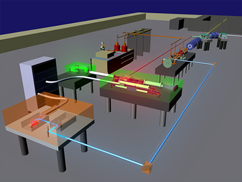
Last February, David Gibson, Christopher Barty and colleagues at the National Ignition Facility and Photon Science Division at Lawrence Livermore National Laboratory (LLNL) published their initial results on a MEGa-Ray source they constructed as groundwork for a beefier machine (2 MeV) in the future. At 2 MeV, such a narrow-bandwidth, high-energy, x-ray source could provide brightness 15 orders of magnitude greater than those produced by synchotrons. The artist rendition of the facility shown in the figure above demonstrates the compact size (a large room) compared to the kilometer-scale rings or linacs conventionally used for generating high energy x-ray beams. Additionally, x-rays of this energy and brightness will find use in nuclear physics and applications such as detection of concealed nuclear material or specific isotope detection and quantification.

So how do you make a MEGa-Ray? By scattering high-intensity laser photons off of a relativistic electron beam (Compton Scattering). In fact, the relativistic electrons are made with a laser as well. The group at LLNL uses matched fiber laser oscillators and fiber-based amplifiers to make the relativistic electrons and the high-intensity scattering light to produce the end product.

Brian Redman from Lockheed Martin and his collaborators, on the other hand, are using light in a very different way- to scan human faces for secure identification and threat-detection. Biometric identification refers to a technique in which a subject can be identified by a unique physical trait or something they physically produce. Some examples are fingerprinting, iris scans, facial scans, and analysis of gait. This topic is particular fascinating to me since human identification is something that the human brain does remarkably well, and for which computers often have trouble. We can identify another person with a great success rate from a far distance based on how they walk, their gait (for a fun gait simulator click here). We have an impeccable ability to identify faces, particularly when we are young- babies can recognize different monkey faces. Therefore one of the directions of research on biometric identification is to improve computational algorithms.

One of Lockheed's specific objectives in their partnership with the FBI is to build a database of facial scans analogous to their database of fingerprints, the Integrated Automated Fingerprint Identification System (IAFIS). I look forward to hearing how Dr. Redman's CLEO talk addresses the optics involved in the facial scans, the use of both 2D and 3D scan information, and the success of the algorithms employed.